To build a low distortion (up to 20KHz) and high output power amplifier requires a ultra low distortion, low impedance output stage with an open loop gain exceeding 1MHz.
To realise such a design, and keep the noise figure as low as possible a large number of design considerations have been considered until a viable design (tested using SPICE simulations) is proposed. This work has taken years of thought and months of simulation and redesign.
The output stage will use MOSFET devices as opposed to bipolar, this has been chosen for the following reasons:-
- The inherent Rds limits the short circuit current sufficiently to permit the use of an external short circuit protection circuit to be used that does not contribute to amplifier distortion.
- The negative temperature coefficient of MOSFET simplifies the design of a thermally stable output stage.
- The higher frequency response permits a tighter feedback loop further reducing distortion.
Bipolar devices are capable of delivering equivalent performance, but with additional complexity, this often is at the expense of non linear audio distortion. Years of listening to bipolar vs MOSFET designs has proved MOSFET’s sound better, although MOSFET devices are more expensive, often require higher idle bias current and are harder to source.
The MOSFET output topology has been carefully considered and over 20 alternate topologies tried, some offer considerable cross over distortion reduction but at the price of difficult driving impedance or poor thermal stability. After months of experimentation, electrical and thermal modeling it has been decided to return to a traditional source follower approach.
Low Noise FET Input
The use of a FET input stage greatly reduces DC offset as it is a voltage amplifier as opposed to current hence input bias currents do not affect DC offsets. The matching of the input FET devices is aided by matched pairs, for this reason the LSK389 has been a popular choice. Sadly the high capacitance of the input, around 20pF greatly limited phase and frequency responses. The newer LSK489 is an ideal choice with only 4pF capacitance and 
The use of a temperature compensated constant current sink and cascaded FET drains yields the following differential topology:-
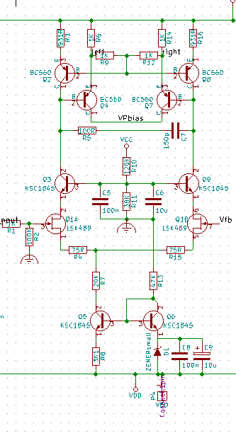
The voltage source is a low noise temperature compensated zenor device at 6.2V. This provides a 2mA sink current through R7. The power rails are +-60V, so the voltage on the source of the LSK489 devices is approximately ")
 -0.6V = 13.8V")
This places a maximum voltage of 27V across LSK489 – Well within it’s design parameters.
The filtering across the reference Zenor diode here is non optimal, the output impedance of the noise across D1 is low and should has a series resistor to reduce noise.
R5 and C7 place a pole at around 3MHz, limiting the differential bandwidth. The final design has a number of zero’s and poles to stabilize the amplifier and produce a favorable bode plot.
The cascoded FET stage also acts to reduce the voltages across the top current mirrors and low impedance drivers Q2, Q4, Q7 and Q8 which can be a very low noise, high frequency bipolar device. BC560C‘s were chosen here as they have suitable high gain.
Care was taken to match transistors in equal gain pairs, although the emitter degeneration reduces the effect of this.


 term is smaller as expected, but in addition the
  and
and  terms are smaller. If we further reduce the gain to 2, by adjusting the feedback resistors we get:-