When designing ultimate high fidelity audio amplifiers thermal stability and cooling become a huge issue. Here I consider a design of a class AB amplifier with a MOSFET output driver stage.
The amplifier is designed to deliver approximately 100W undistorted, this will require a +-45V supply rail. To drive the MOSFET’s a higher supply voltage is required. In this design I have chosen 55V, the driver stage draws 19mA, equating to 2W of power per channel. In addition the output MOSFET’s will require a residual bias current of 60mA, consuming 5.4W. This amounts to 7.4 watts idle per channel, 15W in total at idle.
There is little we can do to reduce this, clever standby logic can reduce this by disabling the output driver when no signal is present, but when in use, and when under a 20W load for example 30W of heat will need to be dissipated.
Passive cooling is preferred over fan noise, an almost perfect high fidelity system be pointless if a fan is producing noise in the background. Passive cooling is vulnerable to poor airflow so thermal monitoring and shutdown is mandatory in such systems to ensure when, for example a record sleeve is placed over the amplifier it does not overheat.
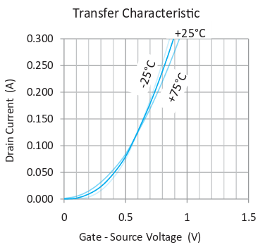
The thermal stability of the output stage also needs careful design, in classical MOSFET output stages the idle bias current is chosen to be the point at which the device is thermally stable. An example of this are the Exicon ECX10N20 devices (see datasheet) where the Vgs temperature coefficient is zero at 110mA and increases beyond this point. Sadly 110mA is far too high, so additional temperature compensation is required to stabilize the devices at a lower idle bias point. The negative temperature coefficient at higher currents protects against short circuit and high temperature failure making these devices extremely rugged:-
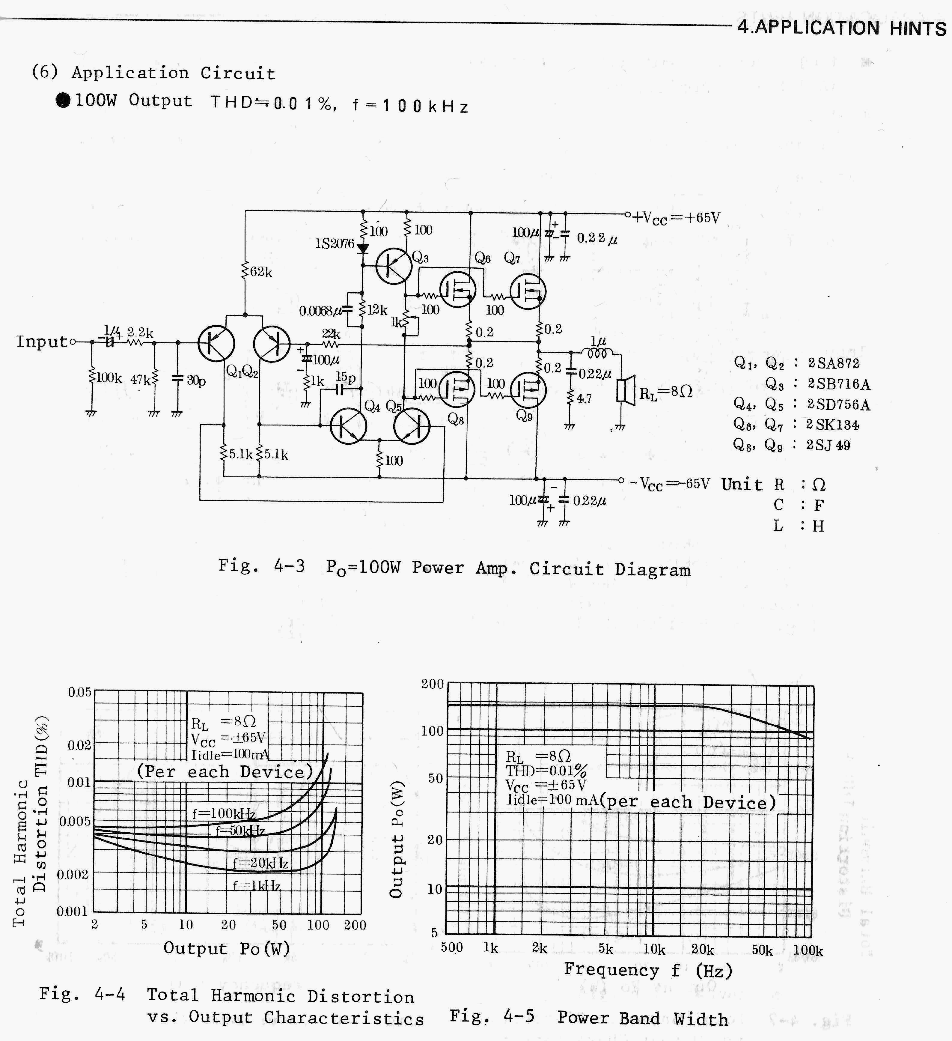
Using such devices has yielded classical MOSFET amplifier designs which have passed the test of time. An Hitachi power MOSFET design was included in their design guides in 1985 which was the basis of the Maplin Electronics 75W amplifier:-
I built a pair of similar amplifiers which sounded great and were bomb proof, continuing to work for over 20 years.
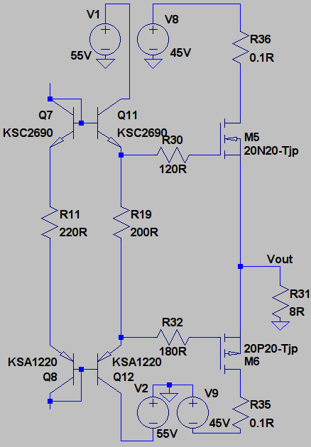
A similar output stage, which turns a current source into a bias voltage that is thermally stable is shown below:-
Transistor Mounting
The heat-sink will have a cooling ability defined as a thermal resistance (
Unfortunately there are other thermal resistances between the actual transistor junction and the heat-sink, which can be reduced to a transistor junction to case resistance and a case to heat-sink resistance:-
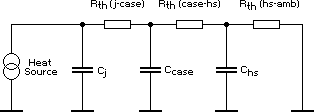
The thermal capacitance 


The table below shows the typical thermal resistance of different materials:-
| Material | Electrical Insulation | Thermal Resistance Wm-1°C-1 | Cost | Notes |
|---|---|---|---|---|
| Mica | 4500 volts/mm | 0.528 | High | Requires silicon paste |
| Sil-Pads | 700 volts/mm | 1.0 | Medium | Easy to use |
| Kapton | 0.9-1.5 | High | Ages under high temperatures |
Kapton is used in many designs, but suffers with lower thermal conductivity and stability over time. Using mica with thermal compound is expensive, difficulty and messy, but is the best solution. For ultimate high fidelity designs we will use mica washers and thermal compound.
Care must be taken not to contaminate any connections with silicon thermal compound as (i) it prevents reliable soldering and (ii) it eventually leads to connector failure if contaminating any connectors.
The final piece of the puzzle is the use of a Vbe multiplier to set the MOSFET bias point. This design has been used in most high fidelity amplifiers to provide some -Ve thermal compensation into the output stages and allow the bias voltage to be easily adjusted:-
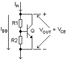
Often R1 or R2 is variable to adjust the bias point of the output FET’s and the transistor is bolted to the output heat sink close to the output devices. The Vbe offset voltage drops as temperature rises ensuring voltage Vce is inversely proportional to the temperature.
The use of a variable resistor for r1/r2 vastly affects reliability and can contribute towards distortion caused by non linear effects in carbon tracks. It is often better to use a select on test approach using fixed metal film resistors. This approach has been adopted in this design.
Finally, the choice of heat sink material is to be considered. It is clear that copper is a far better conductor of heat:-
Thermal Conductivity of Metals
| Material | Thermal Conductivity  | Notes |
|---|---|---|
| Aluminium | 237 | Surface oxidation also increases contact resistance |
| Copper | 401 | Copper is rarely 100% pure - so often this figure is slightly smaller |
| Steel (carbon 1%) | 43 |
From here copper seems ideal. In this design a large copper plate will conduct heat away to the chassis which will be covered in a large aluminium heat sink. Aluminium is far stronger and easier to machine into complex heat sink shapes.