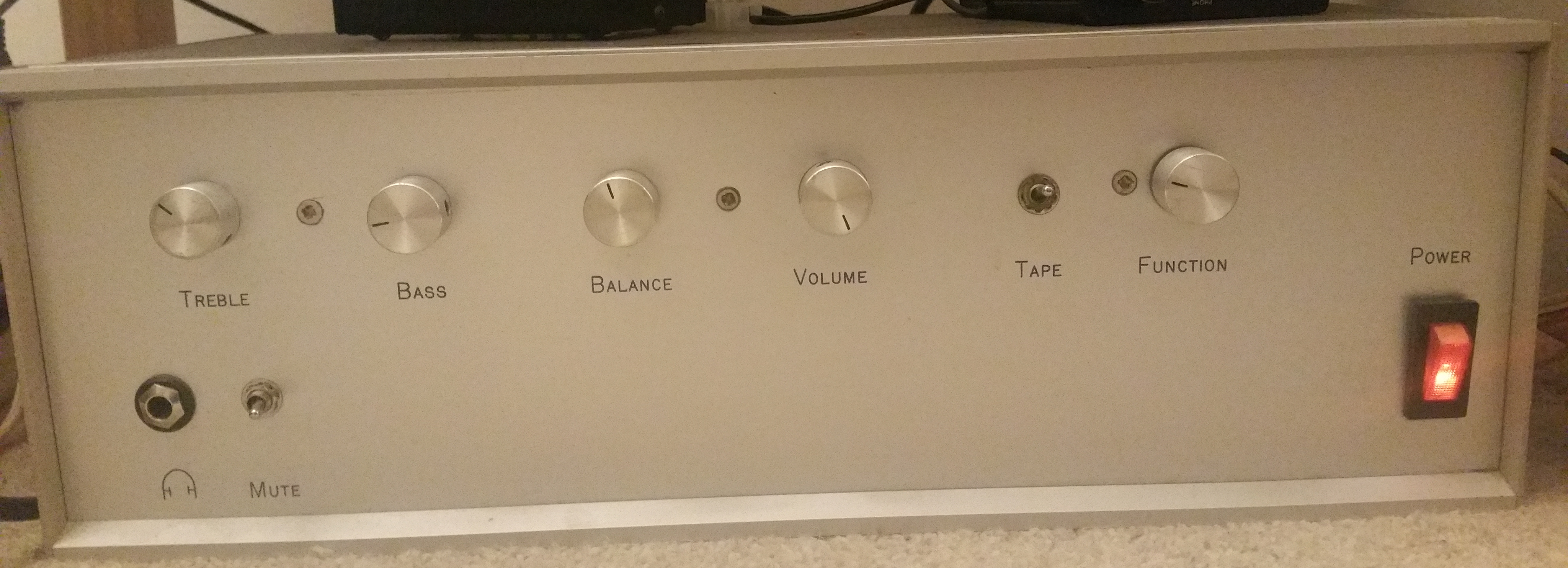
There are countless publications and designs for high-fidelity audio power amplifiers. As an audio engineer I have recently been designing a new power amplifier to replace my 3rd generation amplifier initially built over 25 years ago.
Much discussion has been made on “Square Law” and “Cube Law” amplifiers to reduce harmonic distortion by altering the drives to the output devices.
As an initial study, I simulated the following circuit in LTSpice and extracted a polynomial regression of the input and output data points. This then gives a clear indication of the transfer function. The following circuit:-
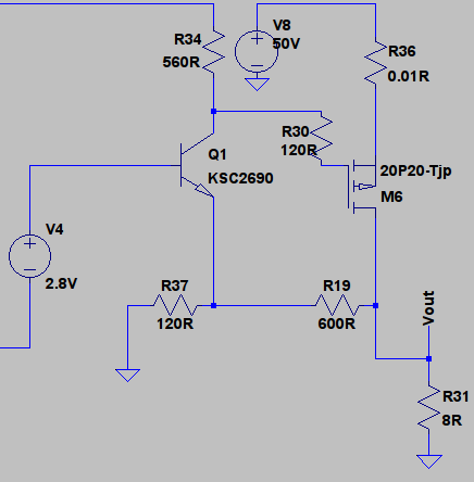
Running a spice simulation followed by a 5th term polynomial regression yielded the following equation:-

The 1.03 offset is unimportant, the 5.09 is the gain of the stage. The unwanted components are the square, cube and quadratic terms. The higher order terms produce greater distortion at higher signal amplitudes.
It is worth comparing this with the equivalent circuit using a MOSFET driver:-
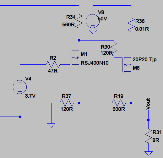
This produced the following polynomial:-

Clearly the 


If we can alter the drive to have -ve
This work progressed to analysing hundreds of MOSFET output stages, the best design based on work suggested by Bob Cordell in his book Bob Cordell “Designing Audio Power Amplifiers”
This design has very low THD, but required additional complexity to the driving VAS stage. The distortion improvements in the output stage were lost in the additional complexity in the VAS driving stage.
The final decision was to use a conventional source following design with 3 pole miller compensation and careful VAS design. Most distortion is generated at +-1V where there s a transconductance imbalance. The initial design will ignore this and allow the feedback to cancel most of this error. The snag with -Ve feedback is it’s performance at higher frequencies, if the frequency response of the VAS stage is insufficient the error at 20KHz will be greater. We will consider the use of local error injection into the driver stage to reduce this error, hence reducing high frequency distortion.